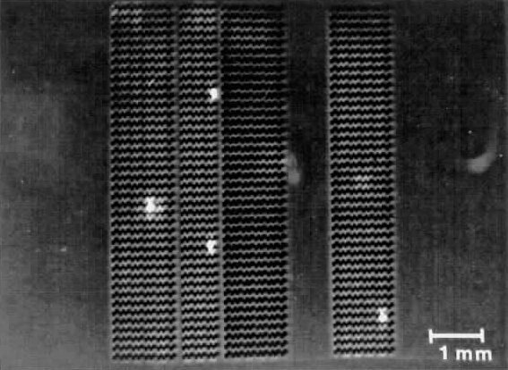
| Electron Beam Analysis of Integrated Circuits and Semiconductor DevicesJerome D. SchickThe Scanning Electron Microscope (SEM) has become an important tool in the characterization and failure analysis of integrated circuits and semiconductor devices. The proliferation of device designs and increasing circuit densities make high spatial resolution analysis techniques necessary. The SEM offers a variety of analytical modes of operation, each contributing unique information regarding the physical and electrical properties of the device or circuit. This discussion will cover Voltage Contrast (VC), Specimen Absorbed Current (SAC), Electron Beam Induced Current (EBIC), and the related Optical Beam Induced Current (OBIC). Each of these techniques requires electrical contact to the device or area of interest and allows electrical stimulus to be applied to the specimen or electrical information to be collected from the specimen.VOLTAGE CONTRASTWhen a sample is examined in the SEM in the Secondary Electron Emission Mode, contrast differences that are caused by localized voltage differences in the specimen may appear in the image. This is called Voltage Contrast, and the contrast arises from alterations in the detected electron signal due to variations in the electric fields in and above the specimen. For example, if a portion of the sample is at a more negative bias than the rest of the sample, this portion of the sample might appear brighter than other similar areas of the sample that are unbiased. This allows the intentional application of various voltage levels to the devicie under SEM examination resulting in an image showing exactly where these voltage levels reside. Figure 1 shows an image of several Aluminum conductors making contact to devices through contact holes. Five volts is applied to these lines, and they appear bright in the SEM image. Notice that one center Aluminum line is dark where it makes contact to the Silicon. This indicates that the Aluminum conductor is open around the perphery of the contact hole, and an electrical defect in the metallization has been located. Subsequent analysis will result in the cause for this failure. |
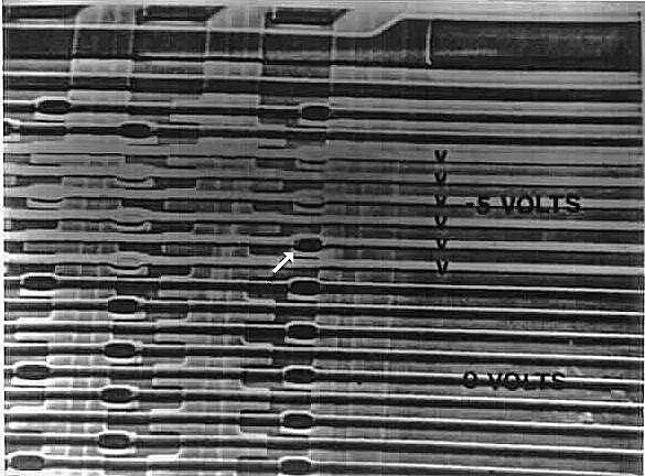
| Figure 1. Voltage Contrast Scanning Electron Microscope image of aluminum conductors with electrically open contact indicated by arrow. |
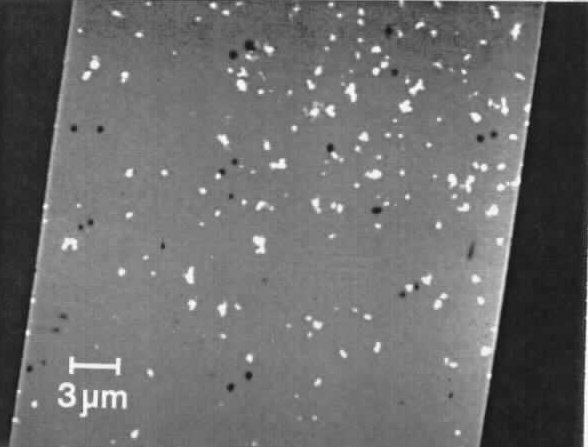
| Measurements may also be carried out in a dynamic mode, where an entire functioning chip is placed in the SEM and the paths of certain voltage levels are traced, or the paths of certain voltage frequencies are traced. Precise timing measurements may also be carried out in a similar way. Special electron detectors are being designed to increase the voltage sensitivity (voltage resolution) in the SEM today. Certain instruments operate as device testers, but are actually Scanning Electron Microscopes operated in the Voltage Contrast Mode with the usual electron microscope features deemphasized.SPECIMEN ABSORBED CURRENTWhen the electron beam of an SEM is absorbed by a sample, a charge build up may occur. The accumulated charge may be either positive or negative, depending on the secondary electron yield of the specimen. If the sample is wired to ground through a current meter, the absorbed charge will flow to ground and the current meter will indicate the degree of electron beam absorption. If the output of the current meter or current amplifier is connected to the input of a video channel, an image may be obtained which shows the portion of the sample electrically connected to the input of the amplifier. If a serpentine metallurgy pattern is connected to a current amplifier in this way. and the entire patters is scanned with the electron beam, the Specimen Absorbed Current image will show the entire metallurgy pattern, unless there is an electrical discontinuity in the pattern separating a portion of the conductor from the connection to the current amplifier. Then the precise location and shape of the discontinuity will be imaged and further physical analysis may be performed.Figure 2 shows an example of locating an open in a dense via connection pattern. After the chain was stressed, it became open, and the interest was in analyzing the failed area. The end of the via chain was connected to the input of a current amplifier and the entire chain was scanned with an electron beam of suitable beam voltage for maximum beam absorption in the metal. The figure indicates the failure, and further analysis showed a thinning of the metal as it dropped over the edge of this particular via hole. |
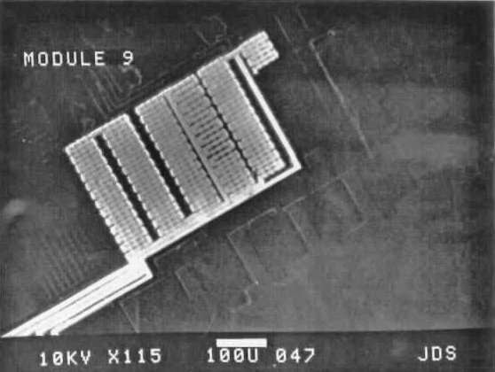
| Figure 2. Broken serpentine conductor pattern with defect located by Specimen Absorbed Current collected from one end of the chain. |
| ELECTRON BEAM INDUCED CURRENTWhen an electron beam is absorbed by a semiconductor material, hole-electron pairs are generated. If these mobile carriers are created within the depletion region of a p-n junction, they are swept out by the existing junction potential, giving rise to an external reverse current. This Electron Beam Induced Current, EBIC, may be amplified and used to obtain information about the junction in which it was generated. Information regarding the location of the true electrical junction within the semiconductor, as well as localized variations in the junction, may be obtained. The reader should keep in mind that it is the depletion region of the junction which causes a current when the mobile carriers are generated. |
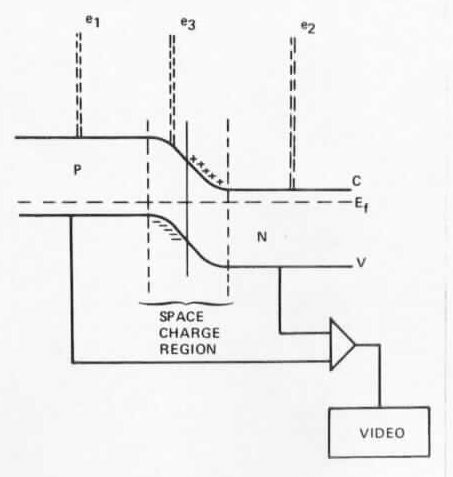
| Figure 3. Band model diagram showing current amplifier wired to a p-n junction for Electron Beam Induced Current measurements. |
| Consider a p-n junction connected in the manner shown schematically in Figure 3 and placed inside a Scanning Electron Microscope. When the electron beam strikes the semiconductor, hole-electron pairs are generated from impurity state transitions as well as from band-to-band transitions. When the amplifier is a low input impedance, high gain current amplifier, there is essentially no external bias placed across the junction. With the beam at e3, or at any place within the space charge region, the current measured is proportional to the electric field at the generation site. With the beam at either e1 or e2, the generated carriers outside the space charge region diffuse randomly until they recombine. These carriers do not contribute to the EBIC being measured. Several authors have treated the generation of these currents theoretically, but the SEM requirements for making EBIC measurements are usually met by incorporating only a few additional requirements on whatever SEM is to be used. The sample must be suitably mounted with electrical connections to both sides of the junction to be studied. These contacts may be electrical needle probes or the sample may be mounted on a header with wire bonds connected to pins. Vacuum feed-throughs with shielded wiring provide proper external connections for a low input impedance, high current gain amplifier whose output is connected to an input channel of the SEM. |
| Figure 4. Electron Beam Induced Current image of an array of transistors with base-collector shorts. Bright areas are the collector-isolation junction areas of defective devices. |
| In Figure 4, the amplifier is connected across the common emitter-base junctions of an array of transistors which had base-collector shorts. The bright areas indicate the defective transistors, and they appear bright because the emitter-base connection to a defective transistor also provides a connection to the collector-isolation junction which then provides an EBIC signal indicating the the defective devices in the array. It can be seen that an understanding of the electrical parameters and the device layout is essential for interpretation of the EBIC results. |
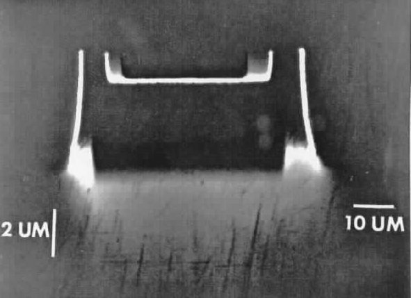
| Figure 5. Electron Beam Induced Current image of a piped transistor obtained by connecting the amplifier across the emitter-base junction. The dark areas are the electrical pipes, and the bright areas are surface depressions resulting from metallurgy removal. |
| EBIC may also be used to locate a defect in an individual transistor. In Figure 5, pipes are located by connection to the emitter-base junction of a piped transistor. The dark spots indicate the areas where the EBIC signal is significantly reduced. This is the location where a pipe exists. When the beam ordinarily excites both the emitter-base junction and the base collector junction from the surface, a uniform signal is obtained. However, if the base dopant is compensated and the emitter contacts the collector, no junction is present, and a reduced signal results. These are highly localized regions, and in this particular case, the pipes can be seen occurring primarily in pairs. The bright areas in this micrograph are associated with depressions on the surface of the device resulting from removal of the metallurgy. These depressions allow the electron beam to reach the junctions more readily causing localized increased EBIC signal. |
| Figure 6. Junctions of an individual transistor obtained by collecting the Electron Beam Induced Current from the emitter-collector connections to the current amplifier. |
| Junctions may also be studied in section in order to obtain vertical information. Junction depths and base widths may be measured by EBIC. Figure 6 shows the vertical structure of a single NPN transistor where the emitter-base junction appears dark and the base-collector junction appears bright. Channel length measurements may be performed on short channel Field Effect Transistors, as well. One major advantage of EBIC is that the measurement is performed on the true electrical junction rather than on a metallurgical result brought about by junction etching or staining. |