The Company:
Kammrath & Weiss, Inc. is a United States Corporation, registered in New York State and owned and operated by Jerome D. Schick. Originally, it was established to do business in the United States on behalf of the German Company of the same name. In 2009 the German Company, Kammrath & Weiss, GMBH, decided to terminate its contract with the USA company, form its own company, and conduct business in the United States through that company. The company still specializes in highly technical and sophisticated peripheral equipment for Scanning Electron Microscopes, Focused Ion Beam Instruments, and other similar laboratory equipment.
The interested reader may investigate the Kammrath & Weiss, GMBH website, and he may survey this and other companies for offerings of equipment that might interest him and solve a technology problem he is pursuing. Although this organizational change was smooth and amicable, the reader is encouraged to contact this present author, Jerome D. Schick, and discuss the possibilities of equipment service as well as equipment purchase and applications in the newly organized environment.
In-FIB Probing:
Recently SEMICONDUCTOR INTERNATIONAL described the importance of the introduction of a probing capability into a Scanning Electron Microscope and a Focused Ion Beam instrument. This, of course, has to do with the device dimensions and the chip density. The size and density of integrated circuits make the probing of individual devices on chips nearly impossible without better viewing of the circuit and finer probe tips with more precise control.
There is a prober system which can be installed in a Focused Ion Beam Instrument. The purpose of this device is to enable probing with four electrical needle probes on an integrated circuit in situ inside the FIB. For a discussion of some outstanding work performed at an Intel Laboratory, CLICK HERE. This is a .pdf file, so you will need Acrobat Reader to read the file. It may take a while to download. Edwin Quijana, Paul Concepcion, and Terence Lacuesta show the slides they used for this fine presentation.
The reader should appreciate the details regarding this work when he considers the size of the individual contacts on the chip and the necessity of contacting four such contacts by the four probes. The probed device is then exercised with a Semiconductor Device Tester to obtain the characteristics for the single transistor. A discussion is also covered in which a failed device is probed and analyzed to determine the cause for failure. Although a detailed discussion is not available with these slides, the reader can follow the work by viewing the slides.
Active Probing:
The term active probing typically refers to the measurement where an active chip is operating and a measurement of some voltage node in the operating chip is measured. Usually the measurement on an internal node using a mechanical probe tip touching the node will load the circuit such that it will be measureably slower or even not function. Active probing utilizes a probe tip with of high series resistance and low input capacitance, sometimes called tip capacitance, such that the Device Under Test (DUT) continues to operate normally even when probed. A probe used for passive probing may have 1 megohm/>10 pf input capacitance. Active probing requires 1 megohm/<1 pf input capacitance. The input sensitivity also requires noise-free amplification such that a FET amplifier very near the probe tip is essential for adequate signal detection. Thus the active probing system requires an active probe tip, a suitable probe arm for holding the tip/FET combination, and a power supply appropriate for driving the amplifier system. The bandwidth of the probing system should be DC to 300 MHz.
Although Kammrath & Weiss has yet to install its first Active Probing System using its Prober System for SEMs and FIBs, the leakage current and capacitance measured with the signal cabling already installed on probing systems is adequate for active probing. Triax signal cables are typically supplied with the four-probe system allowing for the desireable driven shield guard between the signal lead and the grounded shield. Triax cables are essential for low level probing measurements using the typical Semiconductor Parameter Analyzer instrumentation for device characterization inside an electron and/or ion beam system.
Authors from ANALOG DEVICES, Quality Systems, M.B. Ferrara and G.G. Owen described their work in which they performed Active Electron Beam Probing Techniques with an Existing Failure Analysis Process. These authors did not utilize a probing system inside their SEM, but contacted the DUT with socket pins and silver painted contacts. The present author, Jerome D. Schick, has demonstrated the same techniques using probing systems. These probing results are discussed earlier in this site and elsewhere. At this writing, he has not yet demonstrated an Active Probing Measurement using the Kammrath & Weiss Probing System, but is confident of being able to do so. The necessary socket to hold the functioning integrated circuit chip mounted top-side-up on its module has not been selected or designed. The reader should remember that all connections must be made to the chip inside the SEM or FIB in order for the chip to operate. Then the operating chip may be probed with one or more active probe tips.
Another Breakthrough:
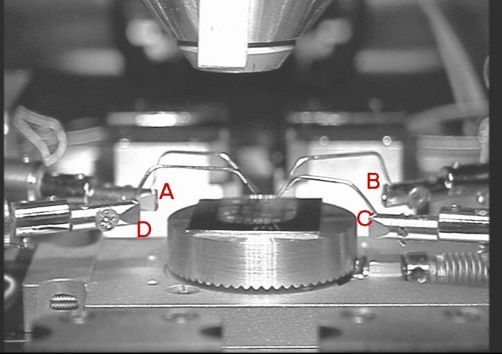
In November of 2003 a first-of-a-kind prober module that can be operated in a FEI 9800 Focused Ion Beam and also in a LEO 1550 Scanning Electron Microscope was installed. The operation for this particular customer is to operate the prober in the FIB, with full X-, Y-, and Z- motions of four independent probe tips, all motions with less than 0.1 micron tip placement accuracy. The prober module may then be removed from the FIB and inserted in the SEM for the same full probing capability. When desired, a sample rotation capability for the SEM may be used to rotate the specimen under the probes. The probing mechanism for the FIB must be of materials that will withstand the harsh, and often chemically reactive, environment in the FIB vacuum chamber. This is not the case in the SEM chamber, but in order for the prober module to be used in BOTH instruments, the more severe case determines the construction of the module.
2010 Status:
In the last few years, although the interest in probing integrated circuits in an electron beam or ion beam instrument has not decreased, the funding for such activities is diminishing. The German Kammrath & Weiss, GmbH company has altered its direction to exclude most efforts in the probing business. Although several advances in techniques were being considered, their marketing emphasizes other metallurgical techniques and accessories. Hopefully the difficult times will begin to improve to allow a return to their broader interests.